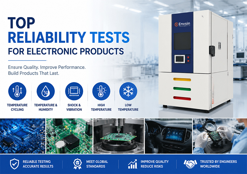
From automotive power chips to 5G processors, semiconductor reliability hinges on one critical variable: temperature. A 2°C deviation during validation can mask latent defects, triggering early-life failures in the field. The answer? Precise, repeatable semiconductor temperature testing. Leading manufacturers trust advanced temperature test chambers to simulate real-world thermal stress. In this guide, we break down essential methods, persistent challenges, and proven best practices — leveraging expertise from Envsin (www.envsin-testchamber.com), a global provider of high-performance environmental test solutions.
1. Key Methods for Semiconductor Temperature Testing
Effective semiconductor temperature testing relies on standardized stress procedures that expose devices to extreme thermal conditions. The most widely adopted methods include:
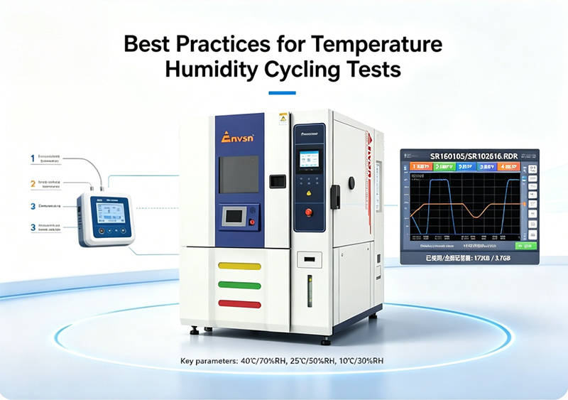
- Thermal Cycling Test (TCT): Alternates between low and high temperatures (e.g., -65°C to +150°C) to assess solder joint fatigue and package integrity. Performed inside a robust temperature test chamber with controlled ramp rates.
- Thermal Shock Test: Subjects components to instantaneous temperature changes (two-zone or liquid-to-liquid) to reveal material weaknesses and delamination risks.
- High-Temperature Operating Life (HTOL): Combines elevated ambient temperature with biased operation to accelerate failure mechanisms and calculate early reliability metrics.
- Low-Temperature Storage & Operation: Verifies functionality at extreme cold conditions, critical for automotive and aerospace semiconductors.
Each method demands an accurate environmental test chamber with advanced control systems. Envsin’s chambers deliver uniform thermal profiles essential for repeatable semiconductor characterization.
2. Common Challenges in Thermal Validation
Despite technological progress, engineers face recurring obstacles that compromise reliability testing outcomes. The main challenges in semiconductor temperature testing include:
- Temperature uniformity & stability: Non-uniform airflow inside the chamber can create hot/cold spots, leading to inconclusive data and overstressing specific DUTs (devices under test).
- Rapid temperature change rates: Many automotive standards (AEC-Q100) require fast transitions (≥15°C/min). Inadequate chambers fail to meet such rates, prolonging test cycles.
- Self-heating effects: Active semiconductors generate internal heat, altering the local temperature. Without proper thermal management (e.g., forced air or cold plates), readings become misleading.
- Condensation & icing: During low-to-high transitions, moisture can condense on sensitive components, causing electrical shorts or corrosion if chambers lack proper purge or dry-air systems.
- Compliance with evolving standards: Meeting JEDEC, MIL-STD, or IEC norms demands traceable calibration and documentation — a burden without integrated data logging.
3. Best Practices to Optimize Temperature Testing
Implementing a robust semiconductor temperature testing strategy eliminates guesswork and boosts throughput. Follow these best practices to achieve world-class results:
✅ Choose the right Temperature Test Chamber
Invest in a versatile temperature test chamber that offers wide temperature range (-70°C to +180°C), fast ramp rates (10–25°C/min), and superior uniformity (±0.5°C). Envsin designs custom environmental test chambers with advanced air distribution and cascade refrigeration — ideal for semiconductor reliability labs. Explore models at www.envsin-testchamber.com.
✅ Implement Real-time Monitoring & Adaptive Control
Use multi-zone sensors and feedback loops to compensate for thermal gradients. Modern chambers from Envsin integrate with lab data systems to automate profile generation, ensuring full traceability for audits.
✅ Manage Self-Heating with Active Thermal Management
For high-power semiconductors, combine chamber air temperature control with local heat sinks or forced convection. This improves correlation between test results and actual application environments.
✅ Regular Calibration & Preventive Maintenance
Schedule annual recalibration of sensors and actuators. Even small drifts in thermocouples can invalidate weeks of reliability testing. Envsin provides on-site calibration support and remote diagnostics to guarantee uptime.
✅ Follow Standardized Test Profiles & Documentation
Leverage pre-programmed profiles compatible with JEDEC JESD22, AEC-Q100, MIL-STD-883. Ensure your environmental test chamber includes robust data logging (CSV/Excel export) for post-test analysis.
Integrating these best practices reduces test variability, shortens time-to-market, and strengthens semiconductor quality assurance. Companies that adopt proactive thermal validation experience up to 40% fewer product returns.
4. Why Partner with Envsin for Semiconductor Temperature Testing?
With over a decade of innovation in environmental simulation, Envsin delivers tailored temperature test chambers designed for semiconductor fabs, OSATs, and R&D labs. Our solutions feature fast transition rates, wide volume flexibility, and energy-saving refrigeration. Every chamber complies with international safety and performance standards, empowering engineers to execute flawless semiconductor temperature testing from early development to high-volume production.
Whether you need a compact benchtop model or a walk-in stability chamber, Envsin’s experts provide custom configurations, remote support, and lifetime calibration services. Visit our website to download datasheets and request a consultation: www.envsin-testchamber.com.
Advanced temperature testing is not just about finding defects — it’s about delivering zero-defect electronics to the market. By combining rigorous methods, proactive challenge-solving, and best-in-class equipment, your semiconductor products earn the reliability that customers trust. Start optimizing your process with the right environmental test chamber partner — Envsin.