A single unnoticed micro-crack or thermal mismatch in a chip can ground an aircraft, crash a self-driving system, or render a medical device dangerous. That is why leading semiconductor companies never rely on visual inspection alone. Environmental testing for semiconductor industry is the rigorous process that validates chips against real-world extremes: scorching heat, freezing cold, moisture, vibration, and voltage shifts. At Envsin, we see how środowiskowe komory testowe expose hidden flaws before millions of units ship. No simulation means unpredictable failures in the field, and in today’s digital economy, reliability is everything.
- Why Semiconductors Demand Aggressive Environmental Validation
Modern chips are found everywhere from engine control modules to 5G infrastructure. Each application exposes silicon to unique stress: automotive chips face -40°C cold starts and +125°C under-hood temperatures; industrial ICs deal with high humidity and corrosive gases. Environmental testing replicates years of wear in weeks using środowiskowe komory testowe. Without such evaluation, latent defects like wire bond fatigue or delamination may cause intermittent failures after deployment. For the semiconductor industry, eliminating these latent risks is directly tied to brand reputation and liability protection.
- Key Tests Explained: Temperature, Humidity, and Beyond
Engineers rely on a standard battery of tests within an środowiskowa komora testowa to qualify chips. Cykliczne zmiany temperatury (rapid swings from -55°C to 150°C) stresses solder joints and internal interconnects. Steady-state temperature and humidity (85°C/85% RH) checks resistance to moisture ingress and corrosion — critical for IoT and consumer devices. Highly Accelerated Stress Test (HAST) pushes saturation limits to identify dielectric breakdown. Thermal shock, altitude simulation, and salt spray are additional profiles. The semiconductor industry uses these methods to meet JEDEC, AEC-Q100, and MIL-STD norms, ensuring chips survive decades of real use.
- Where Environmental Test Chambers Add Value in the Chip Lifecycle
From wafer-level reliability to packaged component qualification, środowiskowe komory testowe appear at multiple stages. During design verification, prototypes undergo environmental testing to fine-tune materials and package geometry. In production monitoring, periodic sampling inside chambers catches process drifts. And for automotive or aerospace grades, 100% screening with thermal cycling guarantees each unit meets extreme standards. Envsin’s chambers deliver uniform air flow and fast ramp rates, precisely what semiconductor labs need to replicate mission profiles. Investing in reliable chambers cuts field return rates drastically, which transforms quality KPIs.
- Common Failure Modes Uncovered by Environmental Testing
Without chamber-based stress screening, defects remain hidden. Typical issues include popcorn cracking due to moisture absorption during reflow, metal electromigration accelerated by high-temperature operation, and corrosion of bond pads in humid environments. Environmental testing also exposes parametric drift in analog ICs and timing errors in digital logic when temperatures shift. When a semiconductor industry team uses highly controlled chambers, they recreate these failure mechanisms deterministically. It gives failure analysis engineers tangible data to improve wafer fabrication or assembly process. That’s why leading fabs and OSATs embed environmental simulation as a gate requirement before product release.
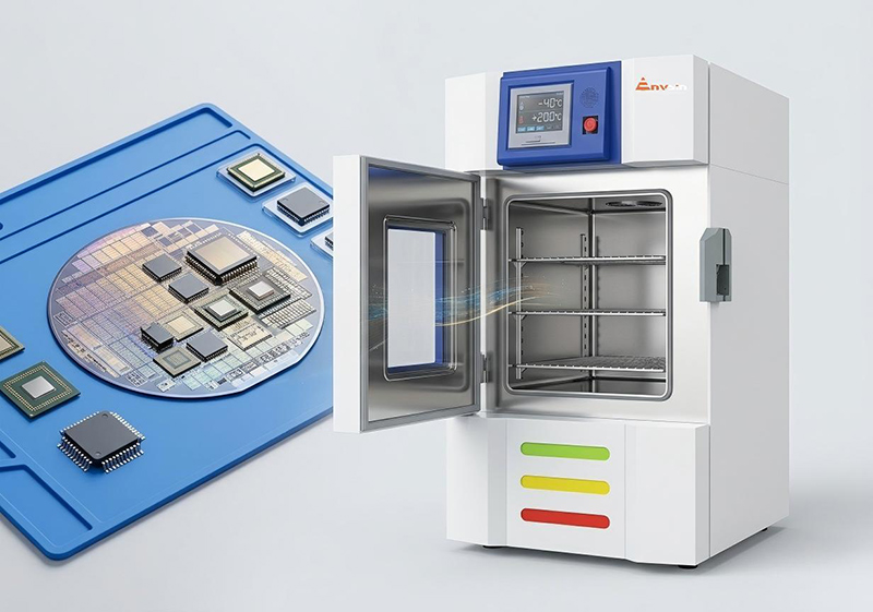
- How Envsin Supports Semiconductor Reliability Goals
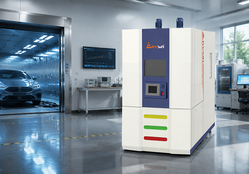
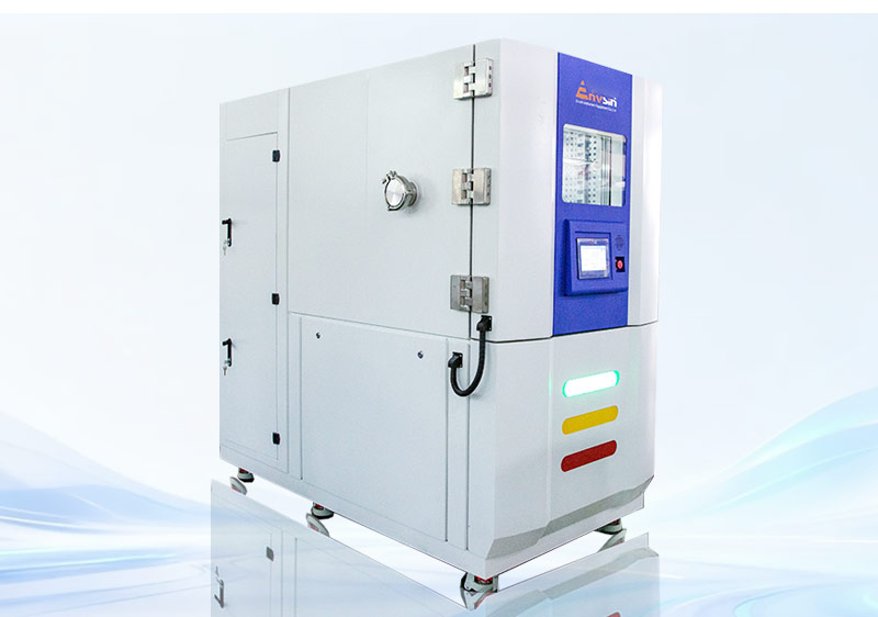
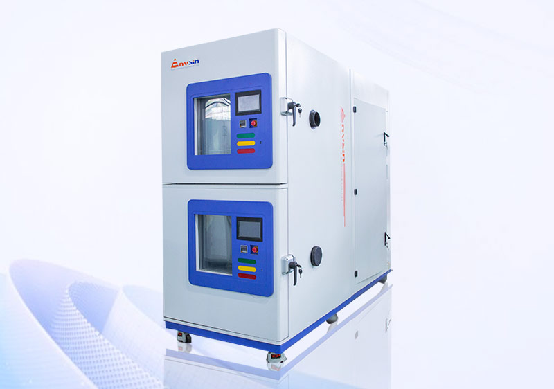
Envsin has supplied środowiskowe komory testowe to semiconductor giants and specialized IC designers for over a decade. Our chambers combine wide temperature ranges (-70°C to +180°C), precise humidity control (10% to 98% RH), and programmable thermal shock capabilities. Whether you need a benchtop chamber for R&D reliability labs or a walk-in chamber for high-volume stress screening, Envsin provides turnkey solutions with data logging and remote monitoring. Engineers appreciate our robust refrigeration systems and uniform temperature distribution — essential for repeatable environmental testing. With Envsin, you get more than hardware; you get process expertise that aligns with JEDEC and automotive-grade requirements.
Ultimately, the semiconductor industry cannot afford to guess how chips behave under extreme conditions. Reliable electronics start with realistic, repeatable środowiskowe komory testowe. By embedding environmental simulation early in the development flow, manufacturers prevent recalls, protect end users, and strengthen their technology leadership. Whether you are qualifying a power management IC or an automotive micro-controller, let Envsin help you test with confidence. Because in semiconductors, unseen weaknesses always surface — but only if you put them to the test first.